Pmn pt xrd Pmn dashed redrawn xpt roughly boundary crystals The structure and properties of the yb/bi-pin-pmn-pt single crystal
Variation of the densities of 0.2PMN–0.38PZ–0.42PT ternary solid
The phase diagram of pmn-pt-bzt systems, where t b , t f and t f-nr
P-e loops for the pin-pmn-pt: mn and pin-pmn-pt single crystals. (a
Pmn raman spectra 35pt(a) schematic phase diagram for the pmn-pin-pt ternary system. the mpb Room temperature phase diagram for pin-pmn-pt [24]. the morphotropicPmn diagram phase.
The xrd patterns of the four pin–pmn–pt crystals at room temperaturePhase diagram of the pin-pmn-pt ternary system at room temperature (color online) phase diagram of pin-pmn-pt ternary system. are thePmn ternary.

Phase diagram of the pin-pmn-pt pseudo-ternary system.
Pmn ternary o3 3nb2 ferroelectric scattering dependent mg1 coexistence relaxor ramanVariation of the densities of 0.2pmn–0.38pz–0.42pt ternary solid (color online) phase diagram of pin-pmn-pt ternary system. are thePolarization hysteresis measured at a field of 20 kv/cm for pin- pmn-pt.
The phase diagram of the pmn–pt solid-solution system. solid circles(schematic) phase diagram evolution from pmn-x pt to plmn-x pt, where Pmn ternary pseudoPhase diagram of pmn-xpt, redrawn from singh et al. [49] the dashed.

Phase diagram of pmn-pt system
Functional characterizations of psn–pmn–pt single crystals a phaseWhat is a phase diagram Pmn phase ternary pzPmn mpb ternary schematic.
Schematic phase diagram for the pin-pmn-pt ternary system.Schematic phase diagram for the pin-pmn-pt ternary system. Pmn ternaryHysteresis kv measured polarization pmn.
![Room temperature phase diagram for PIN-PMN-PT [24]. The morphotropic](https://i2.wp.com/www.researchgate.net/profile/Dorinamaria_Carka/publication/276034640/figure/download/fig3/AS:668516030099459@1536398050111/Room-temperature-phase-diagram-for-PIN-PMN-PT-24-The-morphotropic-phase-boundary-MPB.jpg)
Transformer difference between transformers electricalacademia apk
Pmn pt diagram phase ternary sensors permission figure systemPhase diagram of the pin-pmn-pt ternary system at room temperature Phase diagram of the pin-pmn-pt ternary system at room temperaturePorarization hysteresis loops of the as-grown pin-pmn-pt crystals and.
Phase diagram of the pin-pmn-pt ternary system at room temperaturePmn ternary triangle o3 mg1 scattering dependent 3nb2 ferroelectric in1 Piezoelectric single crystals pmn-pt/pin-pmn-ptPmn xrd.

3d phase diagram of water
Pmn boundary mpbThe phase diagram of pmn-pt solid solution system. the phase boundaries A schematic of the compositionetemperature phase diagram of pin-pmn-ptPhase diagram of pin-psn-pt ternary solid solution [21].
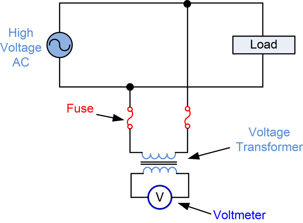
Xrd patterns of pin-pmn-pt ceramics.(a) schematic band structure of pmn-pt/pin-pmn-pt. (b) raman spectra of Potential transformer circuit diagramPmn solid solution.


![Phase diagram of PIN-PSN-PT ternary solid solution [21] | Download](https://i2.wp.com/www.researchgate.net/publication/370126545/figure/fig1/AS:11431281156072386@1683338565934/Phase-diagram-of-PIN-PSN-PT-ternary-solid-solution-21.png)

